


- projects on 2D materials electronics and devices (materials and device aspects)
- both basic nano electronics topics, but also for bio applications like protein/DNA/ single molecule studies
- projects on quantum devices like qubits in 2D ferromagnet devices (from low to room temperature)
- projects on device in situ electron microscopy with single atom resolution (combining microscopy with devices)
- projects on nanoporous 2D membranes (membranes with small < 1 nm holes) for ion, gas transport and other new ideas
| Join our team in 2020 and beyond! We are looking for new graduate students and postdocs to start new projects or expand on the old research themes. See our recent publications for illustration of previous work. |
All photos on these pages are copyright of Drndic lab. For any distribution please contact us for permission.


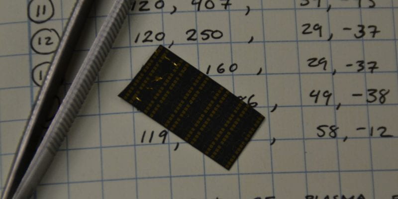
Research in our lab is based on physics and is focused on the exploration of nanoscale and mesoscopic structures with the emphasis on nano electronics, transmission electron microscopy and science of nanoscale & atomic scale systems. The systems that we study include nanoparticles, nanowires, 2D materials and others. For more details, please scroll through our publications. We are experts in transmission electron microscopy, specifically using in situ TEM methods to correlate structure of materials & devices to their properties & function, materials’ synthesis and characterization, low-noise and variable-temperature electrical measurements, fluorescence microscopy, atomic and electric force microscopy, biomolecule measurements with nanopores and so on. We developed the first graphene nanopores for DNA analysis in 2010 as well as new in situ TEM techniques for probing and studying materials at the single atom scale in the recent years. The first transistor measurement inside of the TEM was performed by Dr. Rodriguez-Manzo by carving a graphene sheet into a transistor in situ in the TEM and performing a three-terminal measurement.

We continue to push the frontiers of devices and materials’ applications including the understanding of novel 2D materials, transistors and nanowires, DNA & protein sequencing devices, and the understanding of new electronic phenomena towards quantum information processing. We develop materials and procedures enabling technologies and expanding horizons of physics, chemistry, materials science and nanotechnology. Labs are in David Rittenhouse Laboratory (DRL), the Singh Center for Nanotechnology (Singh Center) and the Laboratory of Research of Structure of Matter (LRSM).
We are seeking motivated graduate students & postdoc to join our effort on the advancement of fundamental nanoscale science, including nanoscale and quantum devices from 2D and other materials, nanopores, 2D materials development, advanced electron microscopy and so on. Please send your interest to Prof. Drndić at drndic@physics.upenn.edu